PWB TECHNOLOGY
- This section is about packaging and interfacing of photonics, in other words: important aspects of the manufacturing process in PIC foundries. It explains the state of the art as well as ELENA’s approach to achieve significant advances in performance, time and cost thanks to a novel technology called Photonic Wire Bonding (PWB).
STATE OF THE ART
- The scalable assembly of hybrid optical systems is considered one of the biggest challenges in photonics manufacturing [1].
- Due to the inherently small optical mode-fields, sub-micron alignment accuracies are required [2]. These requirements cannot be met with “passive” pick-and-place approaches, where the devices are picked with a vacuum tool, for example, and placed at a position determined with the help of a camera.
- Instead, the components must be in operation during assembly, while their alignment relative to each other is optimised by measuring and maximising light coupling through the components [1]. Even worse: While the adhesive for fixing the components cures, they have to be steadily held in the optimal position. With heat-activated adhesives, this is a slow process that takes several minutes [3].
- In general, the active assembly of typical PIC components takes more than ten minutes, even with automated routines [4], and can take up to 45 minutes for a complex transmitter device. Therefore, optical system assembly is the most important cost driver for photonic components to date.
- Besides coupling to an optical fibre, heterogeneous integration of several PICs in one package is extremely important. It allows combining the advantages of different worlds (e.g. gain of a III-V platform with EO control of a LNOI platform) to realise complex devices. The state-of-art methods for heterogeneous integration, such as the flip-chip method or die-bonding, require expensive and complex post-processing steps such as polishing and surface treatments.
ELENA’S PROGRESS BEYOND THE STATE OF THE ART
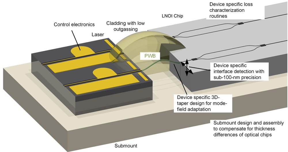
- ELENA will use the concept of Photonic Wire Bonding (PWB). This technology is proprietary to ELENA partner Vanguard Automation and provides a universal solution for coupling LNOI to other PICs (Figure 1) as well as single-mode fibres.
- PWB exploits advanced three-dimensional (3D) nano-printing of single-mode interconnect waveguides between coarsely pre-positioned elements, thereby enabling highly efficient interfaces between waveguides of vastly different mode-field profiles in a fully automated process.
- PWB enables cost-effective hybrid integration of different PICs in a single package for advanced and compact high-end devices where, for example, LNOI chips will allow efficient and fast manipulation of light, and InP chips will provide lasers and photodetectors.
- It is important to note that LNOI ‒ although it is one of the most capable platforms in electronic controlling and routing of light within a chip ‒ does not intrinsically possess optical gain. Therefore, components such as lasers, photodetectors and amplifiers are not possible directly with LNOI.
- Thus, low-cost interfacing between III-V based photonic chips and LNOI significantly increases its scope by hybrid integration of optical sources and detectors within the same optical package, resulting in a significant increase in system compactness and functionality as well as a reduction in cost.
- The PWB technology requires no post-processing on the chip surface and no active pre-alignment. It has been developed to the point where it can be used to realise high-performance photonic multi-chip modules such as an eight-channel transceiver that combines silicon photonic modulators and InP lasers in a hybrid optical assembly [5] (Figure 2). The low-loss heterogeneous integration of InP and LNOI chips is in particular important for ELENA’s prototype for tunable lasers.

Figure 2: An 8-channel transmitter fabricated with the Photonic Wire Bonding (PWB) technology to interconnect various photonic components. Inset (1): Micrograph of a PWB connecting an InP laser array to a SOI chip. Inset (2): Micrograph of two PWBs connecting an SOI chip to single-mode fibres (SMF). Image source: [5]
- The ability to interface photonic chips with electronic circuitry and optical components is key to the industrialisation of PIC devices. Due to the high stability of LiNbO3 crystals in ambient air, hermetic packaging is not always required, which significantly simplifies the integration. Further advantages of this packaging concept are
- Direct wire bonding of PIC chips to test Printed Circuit Boards (PCBs) is planned for end-user demonstrators in ELENA.
- Hybrid assembly of optical systems is considered a very promising approach to create photonic devices in many areas, ranging from optical communication to sensing and quantum applications.

Figure 3: The concept of Photonic Wire Bonds (PWB), illustrated for a modulator chip as used in ELENA
(a) Photonic chips and optical fibres are mounted on a common carrier and embedded into a photosensitive photoresist. Photonic wire bonds are then written in the volume of the resist by two-photon polymerization using a femto-second (fs) laser. The wire bonds can have arbitrary three-dimensional shapes. This eliminates active alignment even for nanoscale single-mode waveguides and enables perfect matching of mode-field sizes. (b) Example electron microscopy image of two interfaces, in this case Silicon-on-Insulator (SOI) chips connected with PWB.
CURIOUS TO LEARN MORE ABOUT PWB ?
- All devices are immersed into a liquid polymer that also serves as immersion medium for a high-NA objective lens. The device facets are then localized with sub-100 nm precision using different machine vision techniques integrated into a lithography system. Using the device positions, a trajectory is calculated that connects the mode-fields of the two optical components with optimal coupling loss. A waveguide is then structured along the trajectory into the liquid polymer by scanning a focused femto-second laser causing two-photon absorption. In addition, tapers adapting different mode field sizes can be implemented by altering the cross-section of the waveguide.
- After the 3D-printing process, the remaining polymer is dissolved in developer and the PWB is cladded in a curable polymer that protects the connection from harsh environmental conditions and adjusts the refractive index contrast to ensure single-mode operation of the PWB for wavelengths in the range of 1250 nm to 1650 nm. The PWB technique is suitable for both edge-coupled devices and adiabatically coupled devices.
- Depending on the device type involved, cycling times below 10 s per optical interconnect are possible with losses down to below 1 dB [8]. In addition, the fabrication of PWB at facets that are tilted with respect to the waveguide is possible to reduce reflection at the device interface. Thanks to the software-defined 3D-nanoprinting, the same lithography tools can fabricate in-situ freeform lenses onto the chip or fibre array facets [9].
FURTHER READINGS
- T. Baehr-Jones et al., Nat. Photonics, 2012, doi: 10.1038/nphoton.2012.66
- P. O’Brien et al, Silicon Photonics III, Springer Berlin Heidelberg, 2016, doi: 10.1007/978-3-642-10503-6_7
- “EPO-TEK ® H20S Technical Data Sheet For Reference Only Electrically Conductive, Silver Epoxy for Die Stamping.”
- G. B. Preve, Silicon Photonics III, Springer Berlin Heidelberg, 2016, doi: 10.1007/978-3-642-10503-6_8
- M. R. Billah et al., Optica, 2018, doi: 10.1364/OPTICA.5.000876
- R. Jones et al., IEEE Nanotechnol. Mag.,2019, doi: 10.1109/MNANO.2019.2891369
- Mekis et al., Topics in Applied Physics, 2016, doi: 10.1109/ECOC.2017.8346187
- M. Blaicher et al., Light: Science & Applications, 2020, doi: 10.1038/s41377-020-0292-1
- Dietrich et al., Nature Photonics, 2018, doi: 10.1038/s41566-018-0133-4

