LNOI TECHNOLOGY
PICs – TECHNOLOGICAL DRIVERS OF THE DECADE


LNOI ‒ A VERSATILE PIC PLATFORM FOR THE FUTURE


ELENA’S LNOI PIC PLATFORM AND BUILDING BLOCKS (BBs)
CSEM’s LNOI PIC Platform


| Property | Value |
|---|---|
| Wafer cut | x |
| Refractive index (ordinary) | 2.21 (@ 1550 nm) |
| Refrafctive index (ex-ordinary) | 2.13 (@ 1550 nm) |
| Bandgap | 4.9eV |
| Transparency window | 350nm − 5.5 𝜇𝑚 |
| Property | Value |
|---|---|
| EO coefficient | r33 = 31 𝑝𝑚/𝑉 |
| 𝜒^((2)) nonlinearity | 3 × 10⁻¹¹ m/V |
| 𝜒^((3)) nonlinearity | 1.6×10⁻²¹ 𝑚2 𝑉−2 |
| Piezoelectric coefficient | d33 = 6.0 × 10⁻¹² C/N |
ELENA’S LNOI BUILDING BLOCKS (BBs)
- ELENA will develop a set of standard BBs with high reliability and yield that can be monolithically integrated and combined in a large variety of PIC designs and applications.
- These BBs will be available to entities outside the consortium via the Process Design Kit (PDK), the industry’s standard method of accessing PIC foundries.
- LNOI photonics technology to be offered as multi-project wafer (MPW) foundry service to the industry
")
-2")
Active BBs
| Building Block | Main target specifications | |
|---|---|---|
| Fast phase shifter |  |
|
| Mach-Zehnder (MZ) modulators | 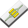 |
|
| Mach-Zehnder (MZ) modulators |  |
|
| Tunable cavities |  |
|
| Variable optical couplers | 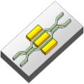 |
Passive BBs
| Building Block | Main target specifications | |
|---|---|---|
| Edge coupler | 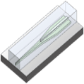 |
|
| Grating coupler | 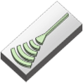 |
|
| Multimode interference coupler (MMI) | 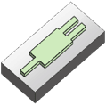 |
|
| Directional coupler | 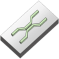 |
|
| Y-junction | 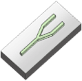 |
|
| Crossings |  |
|
| Resonators |  |
|
| Arrayed Waveguide Grating (AWG) |  |
LNOI VS BULK LITHIUM NIOBATE TECHNOLOGY

Figure : Traditional bulk lithium niobate modulators with ion – diffusion/proton exchange waveguide technology VS Integrated lithium niobate on insulator (LNOI) modulators created with RIE etched thin film waveguide technology
- So far, the industrial success of lithium niobate in the photonics domain has mainly been limited to devices made from bulk LiNbO3 crystals in the form of free-space or fibre-coupled components.
- However, the landscape has changed thanks to recent developments in bonding thin single-crystal LiNbO3 films onto silicon substrates (LNOI).
- This opens up new opportunities to explore the benefits of LNOI for PICs, such mas cost reduction, manufacturability and improved integration into PICs.
LNOI VS OTHER PIC PLATFORMS
")
| Property | InP | Si | SiN | LNOI |
|---|---|---|---|---|
| Transparency window | 0.9 to 2 µm | 1.1 to 8 µm | 0.25 to 8 µm | 0.3 to 5.5 µm |
| Propagation losses | 1.5 to 3 dB/cm | 0.1 to 3 dB/cm | 0.01 to 0.1 dB/cm | < 0.1 |
| Two-photon absorption | High | High | Very low | Very low |
| Electro-optic coefficient | Not intrinsic | Not intrinsic | - | High (31pm/v) |
| Optical gain | Yes | - | - | - |
| Detectors | Yes | Yes | - | - |
| Industry status | Ramping up | High Volume | Low-volume production | No foundry in Europe yet |
- At present (2022), several European foundries offer PIC platforms based on silicon (Si), silicon nitride (SiN) and indium phosphide (InP). Each of these photonic materials offers different and often unique functionalities.
- Currently, there is no commercial foundry for LNOI PICs anywhere in the world, but this may soon change.
- ELENA will fill this gap in Europe and hence represents a timely answer to the market demands and an important contribution to maintain Europe’s lead in high-end photonics technologies throughout the next decade.
LNOI PHOTONICS, AN ENABLING TECHNOLOGY
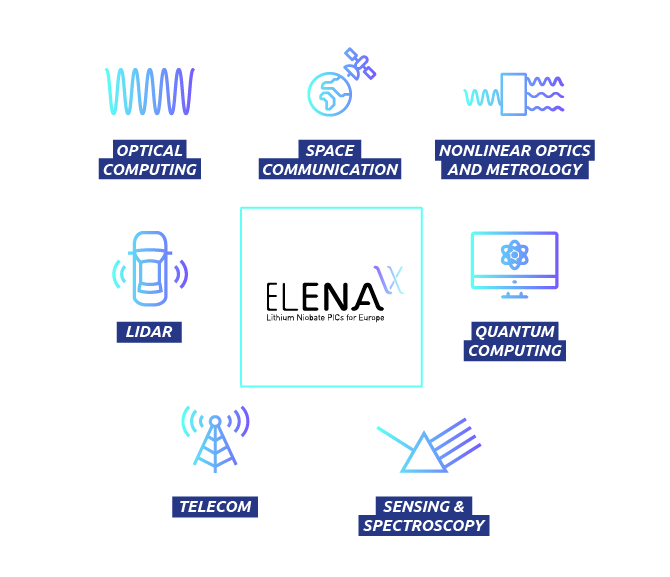
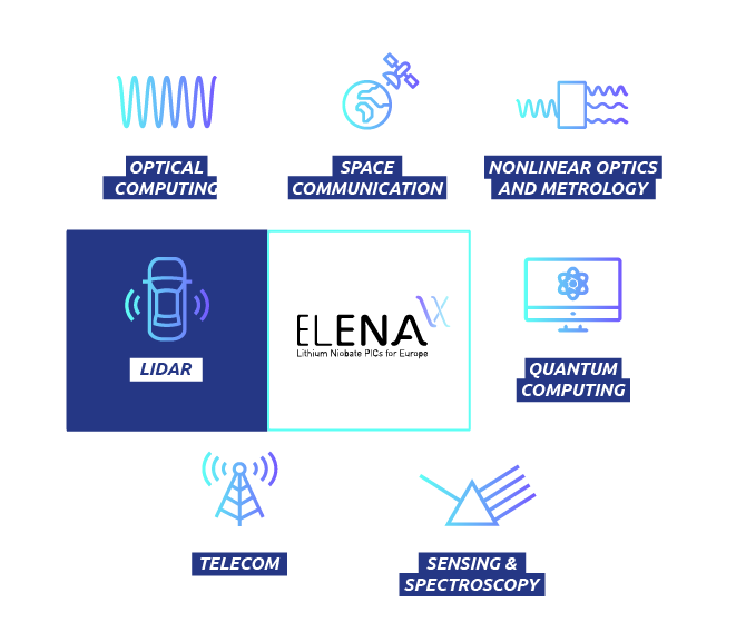
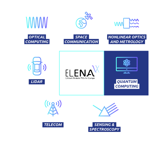
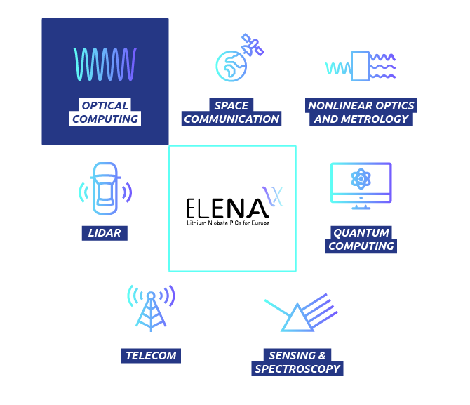
The LNOI platform is ideal for:
FMCW LIDAR:- Fast (< 1ns) tunable laser (EO Vernier Filter)
- Narrow linewidth: ultrahigh resolution (low-loss LNOI waveguides implemented in external-cavity hybrid lasers)
- Multi-wavelength generation [1 - PICs APPLICATIONS]
- Non-mechanical fast beam steering
- Fast, compact, and low-loss EO phase shifters
- Low voltage and low power consumption compared to thermal tuning
- No thermal parasitic crosstalk
The LNOI platform is ideal for:
- Photonic engines [J1 - Journal Publications] for quantum control in atomic-based quantum systems such as: ion trapping, optical lattices, atomic clocks, NV (578 nm) and SV- (737 nm) centers.
- These atomic systems (Ca+ 729 nm, Rb 795 nm, etc.) operate in visible and NIR, unreachable in other PIC platforms.
- Controlling these atomic systems requires ultra-fast pulse generation on demand.
- Pure phase modulation (no spurious amplitude modulation).
- Quantum communication and QKD:
- Entangled photon pair generation through SPDC
- Ultrafast modulation and polarization control
- EO gating and interferometer
- Photonic-based quantum computing (continues variables (CV), Boson sampling, cluster states, etc.) :
- Entangled photon pair generation through SPDC
- Programmable MZI mesh using EO effect
- Low loss
- Pure phase modulation (no spurious amplitude modulation)
The LNOI platform offers many possibilities for optical computing:
- 2nd order nonlinearity and PPLN waveguides: enable various wavelength conversion and generation scenarios envisioning the optical version of bipolar transistors.
- Wide transparency window: enables efficient optical signal manipulations in a wide spectrum which is of great importance for photonic engines (more compact at shorter wavelengths).
- Ultra-fast and low-power EO modulators: allow for brisk optical signal modulation, filtering, and interleaving.
- High-quality passive and active resonators and low-loss waveguides: enable various delay line architectures with agile tuning, crucial for alleged optical processors and agile delay line.
- Neuromorphic computing requiring large-number on-chip component integration: could benefit from low-loss and low-power building blocks and nonlinear properties of the LNOI platform.
- Programmable photonics engines: reconfigurable MZI mesh array, wavelength conversion, etc.
- CMOS-level operating active components: while enabling fast tunable lasers, considerably facilitate the integration of PIC electronics, which is paramount for optical computation.
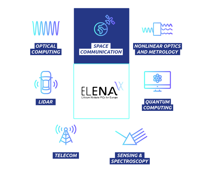
LNOI PICs could enhance space communication in various aspects:
- Low-power, low-weight PICs that can operate across a broad spectrum could vastly expand the space communication links while enabling low operating costs and flexible deployment.
- Ideal for intra-payload, satellite-to-satellite and satellite-to-ground communication.
- LiNbO3 is dialectic and intrinsically compatible with harsh environments (high temperatures, high radiation, EM interference, etc.).
- LNOI PICs could handle high powers which are of great importance for free-space communication.
- LIDARs based on LNOI PICs offer fast multispectral functionality thanks to the implementation of fast EO modulators and their wide transparency window.
- Integration of LNOI PICs with electronics is essential for most space applications; CMOS-level operation modulators in the platform facilitate system integration as well as deployment and control.
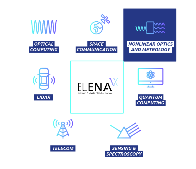
Intrinsic 2nd and 3rd order nonlinearities of LNOI provide a rich toolbox for nonlinear photonics and metrology applications:
- Periodically poled lithium niobate (PPLN) waveguides provide on-chip wavelength conversion (second harmonic generation (SHG), sum frequency generation (SFG), difference frequency generation (DFG), spontaneous parametric down conversion (SPDC), etc.).
- Squeezed light states, entangled photon sources, and measurements below standard quantum limit (SQL) are examples that could benefit from the intrinsic nonlinear properties of the LNOI platform.
- Nonlinear wavelength generation for new wavelength ranges in NIR and visible using SHG and SFG will be instrumental in enhancing applications such as OCT, holography and RGB engine, Raman spectroscopy etc.
- Nonlinear wavelength generation for mid-IR using DFG processes for gas sensing, security, and environment monitoring.
- Ultra-wide and stable frequency comb generation (either Kerr or EO combs).
- Optical self-stabilisation of frequency combs, mode-lock lasers, and supercontinuum sources through f-2f locking scheme [7 - Nonlinear Building Blocks and PPLN (SHG etc.)]
- Stabilising lasers by locking to atomic clocks enabling ultra-precise metrology tools using SHG and SFG.
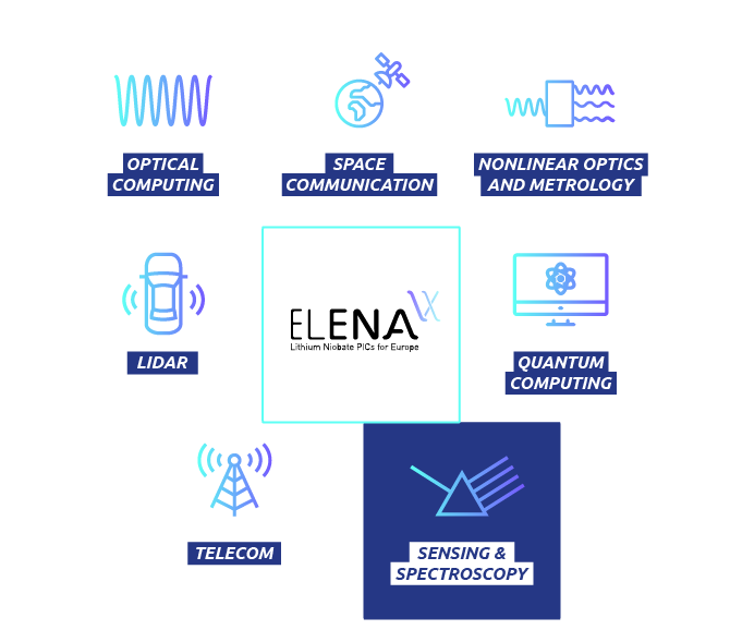
The advantages of LNOI PIC platforms in the field of sensor technology are manifold :
- Multi-wavelength operation (thanks to the wide transparency window from visible to NIR) are interesting for biomonitoring (500 – 1000 nm) and Raman spectroscopy (785 nm) to Mid-IR for gas sensing and environmental monitoring (CO2 at 2, 2.7, 4.8 um, Methane at 3.3 um, etc.) as well as food and water quality monitoring.
- New method of generating light in the above-mentioned wavelengths through nonlinear processes extending InP chip-based lasers (~1550 nm) to other wavelengths.
- Fast and efficient electrical manipulation of optical light-on-chip through various modulation scenarios from thermal to electro-optical for full lab-on-chip systems.
- The possibility to have suspended waveguide structures, strong piezoelectric effects and low loss waveguides make LNOI PICs ideal for opto-mechanical sensing, pressure sensing, and gyros, all deployable with low cost and ease in operation.
- Low-loss waveguides in multiple different thickness enable evanescent field sensing.
- On-chip optical frequency comb spectroscopy (e.g. astrocombs for exoplanet detection, [2 - PICs APPLiCATIONS]).
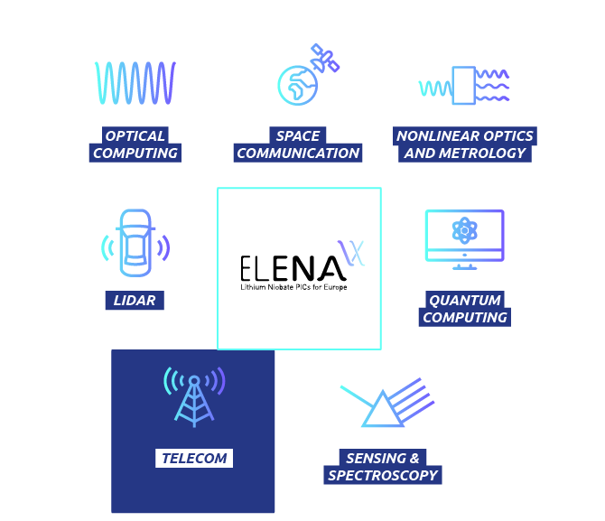
LNOI will primarily serve for telecommunication:
- Ultra-high-speed transmitters: Beyond 400Gbit/s data rates are promised with ultra-fast EO modulators.
- Multi-wavelength operation (including wavelength generation) for coherent dense wavelength division multiplexing (DWDM).
- New wavelength windows are unlocked by this platform by nonlinear conversion of C-band to L-band and S-band using PPLN waveguide.
- CMOS level operation will simplify the transceivers’ architecture and PIC-IC co-integration.
- Low weight, high optical power handling, low power consumption and ultra-fast modulators, and facilitated integration with electronics will position LNOI as the platform of choice for embedding in daily-life tools, office, and residential spaces, making the internet of things ubiquitous.
- High-quality tunable filters and MUX/DMUX units introduces LNOI as a versatile platform for DWDM.
- Integrated EO polarization controllers add a new dimension for on-chip data link engineering with a potential to double the bandwidth.
Here are the links to the three references in the mouse-overs: LIDAR: [1] – PICs Applications; SENSING & SPECTROSCOPY: [2] – PICs Applications; NONLINEAR OPTICS AND METROLOGY: [7] – Nonlinear Building Blocks and PPLN (SHG etc.)
FURTHER READINGS
- Xu and X. Cai, “Advances in integrated ultra-wideband electro-optic modulators [Invited],” Opt. Express, vol. 30, no. 5, p. 7253, Feb. 2022, doi: 10.1364/OE.449022.
- D. Zhu et al., “Integrated photonics on thin-film lithium niobate,” Adv. Opt. Photon., vol. 13, no. 2, p. 242, Jun. 2021, doi: 10.1364/AOP.411024.
- M. Zhang, C. Wang, P. Kharel, D. Zhu, and M. Lončar, “Integrated lithium niobate electro-optic modulators: when performance meets scalability,” Optica, vol. 8, no. 5, p. 652, May 2021, doi: 10.1364/OPTICA.415762.
- M. Zhang, C. Wang, P. Kharel, D. Zhu, and M. Lončar, “Integrated lithium niobate electro-optic modulators: when performance meets scalability,” Optica, vol. 8, no. 5, p. 652, May 2021, doi: 10.1364/OPTICA.415762.
- S. Saravi, T. Pertsch, and F. Setzpfandt, “Lithium Niobate on Insulator: An Emerging Platform for Integrated Quantum Photonics,” Advanced Optical Materials, vol. 9, no. 22, p. 2100789, Nov. 2021, doi: 10.1002/adom.202100789.
- Y. Qi and Y. Li, “Integrated lithium niobate photonics,” Nanophotonics, vol. 9, no. 6, pp. 1287–1320, Apr. 2020, doi: 10.1515/nanoph-2020-0013.
- M. Rusing, P. O. Weigel, J. Zhao, and S. Mookherjea, “Toward 3D Integrated Photonics Including Lithium Niobate Thin Films: A Bridge Between Electronics, Radio Frequency, and Optical Technology,” IEEE Nanotechnology Mag., vol. 13, no. 4, pp. 18–33, Aug. 2019, doi: 10.1109/MNANO.2019.2916115.
- A. Boes, B. Corcoran, L. Chang, J. Bowers, and A. Mitchell, “Status and Potential of Lithium Niobate on Insulator (LNOI) for Photonic Integrated Circuits,” Laser & Photonics Reviews, vol. 12, no. 4, p. 1700256, Apr. 2018, doi: 10.1002/lpor.201700256.
- G. Poberaj, H. Hu, W. Sohler, and P. Günter, “Lithium niobate on insulator (LNOI) for micro-photonic devices,” Laser & Photon. Rev., vol. 6, no. 4, pp. 488–503, Jul. 2012, doi: 10.1002/lpor.201100035.
- E. L. Wooten et al., “A review of lithium niobate modulators for fiber-optic communications systems,” IEEE J. Select. Topics Quantum Electron., vol. 6, no. 1, pp. 69–82, Jan. 2000, doi: 10.1109/2944.826874.
- Xu and X. Cai, “Advances in integrated ultra-wideband electro-optic modulators [Invited],” Opt. Express, vol. 30, no. 5, p. 7253, Feb. 2022, doi: 10.1364/OE.449022.
- M. Zhang, C. Wang, P. Kharel, D. Zhu, and M. Lončar, “Integrated lithium niobate electro-optic modulators: when performance meets scalability,” Optica, vol. 8, no. 5, p. 652, May 2021, doi: 10.1364/OPTICA.415762.
- P. Kharel, C. Reimer, K. Luke, L. He, and M. Zhang, “Breaking voltage–bandwidth limits in integrated lithium niobate modulators using micro-structured electrodes,” Optica, vol. 8, no. 3, p. 357, Mar. 2021, doi: 10.1364/OPTICA.416155.
- N. Boynton et al., “A heterogeneously integrated silicon photonic/lithium niobate travelling wave electro-optic modulator,” Opt. Express, vol. 28, no. 2, p. 1868, Jan. 2020, doi: 10.1364/OE.28.001868.
- A. N. R. Ahmed, S. Shi, S. Nelan, A. J. Mercante, P. Yao, and D. W. Prather, “Low-voltage modulators using thin-film lithium niobate,” in Optical Interconnects XX, San Francisco, United States, Feb. 2020, p. 27. doi: 10.1117/12.2542458.
- A. N. R. Ahmed, S. Shi, A. Mercante, S. Nelan, P. Yao, and D. W. Prather, “High-efficiency lithium niobate modulator for K band operation,” APL Photonics, vol. 5, no. 9, p. 091302, Sep. 2020, doi: 10.1063/5.0020040.
- A. N. R. Ahmed, S. Nelan, S. Shi, P. Yao, A. Mercante, and D. W. Prather, “Subvolt electro-optical modulator on thin-film lithium niobate and silicon nitride hybrid platform,” Opt. Lett., vol. 45, no. 5, p. 1112, Mar. 2020, doi: 10.1364/OL.381892.
- C. Wang, M. Zhang, M. Yu, R. Zhu, H. Hu, and M. Loncar, “Monolithic lithium niobate photonic circuits for Kerr frequency comb generation and modulation,” Nat Commun, vol. 10, no. 1, p. 978, Dec. 2019, doi: 10.1038/s41467-019-08969-6.
- A. Honardoost, F. A. Juneghani, R. Safian, and S. Fathpour, “Towards subterahertz bandwidth ultracompact lithium niobate electrooptic modulators,” Opt. Express, vol. 27, no. 5, p. 6495, Mar. 2019, doi: 10.1364/OE.27.006495.
- M. He et al., “High-performance hybrid silicon and lithium niobate Mach–Zehnder modulators for 100 Gbit s−1 and beyond,” Nat. Photonics, vol. 13, no. 5, pp. 359–364, May 2019, doi: 10.1038/s41566-019-0378-6.
- C. Wang, M. Zhang, B. Stern, M. Lipson, and M. Lončar, “Nanophotonic lithium niobate electro-optic modulators,” Opt. Express, vol. 26, no. 2, p. 1547, Jan. 2018, doi: 10.1364/OE.26.001547.
- C. Wang et al., “Integrated lithium niobate electro-optic modulators operating at CMOS-compatible voltages,” Nature, vol. 562, no. 7725, pp. 101–104, Oct. 2018, doi: 10.1038/s41586-018-0551-y.
- A. Rao and S. Fathpour, “Compact Lithium Niobate Electrooptic Modulators,” IEEE J. Select. Topics Quantum Electron., vol. 24, no. 4, pp. 1–14, Jul. 2018, doi: 10.1109/JSTQE.2017.2779869.
- A. J. Mercante, S. Shi, P. Yao, L. Xie, R. M. Weikle, and D. W. Prather, “Thin film lithium niobate electro-optic modulator with terahertz operating bandwidth,” Opt. Express, vol. 26, no. 11, p. 14810, May 2018, doi: 10.1364/OE.26.014810.
- M. R. Escalé, D. Pohl, A. Sergeyev, and R. Grange, “Extreme electro-optic tuning of Bragg mirrors integrated in lithium niobate nanowaveguides,” Opt. Lett., vol. 43, no. 7, p. 1515, Apr. 2018, doi: 10.1364/OL.43.001515.
- N. Courjal et al., “Lithium Niobate Optical Waveguides and Microwaveguides,” in Emerging Waveguide Technology, K. Y. You, Ed. InTech, 2018. doi: 10.5772/intechopen.76798.
- A. J. Mercante, P. Yao, S. Shi, G. Schneider, J. Murakowski, and D. W. Prather, “110 GHz CMOS compatible thin film LiNbO3 modulator on silicon,” Opt. Express, vol. 24, no. 14, p. 15590, Jul. 2016, doi: 10.1364/OE.24.015590.
- G. T. Reed, G. Mashanovich, F. Y. Gardes, and D. J. Thomson, “Silicon optical modulators,” Nature Photon, vol. 4, no. 8, pp. 518–526, Aug. 2010, doi: 10.1038/nphoton.2010.179.
- D. Janner, D. Tulli, M. García-Granda, M. Belmonte, and V. Pruneri, “Micro-structured integrated electro-optic LiNbO 3 modulators,” Laser & Photon. Rev., vol. 3, no. 3, pp. 301–313, Apr. 2009, doi: 10.1002/lpor.200810073.
- S. Haxha, B. M. A. Rahman, and K. T. V. Grattan, “Bandwidth estimation for ultra-high-speed lithium niobate modulators,” Appl. Opt., vol. 42, no. 15, p. 2674, May 2003, doi: 10.1364/AO.42.002674.
- Luke, P. Kharel, C. Reimer, L. He, M. Loncar, and M. Zhang, “Wafer-scale low-loss lithium niobate photonic integrated circuits,” Opt. Express, vol. 28, no. 17, p. 24452, Aug. 2020, doi: 10.1364/OE.401959.
- B. Desiatov, A. Shams-Ansari, M. Zhang, C. Wang, and M. Lončar, “Ultra-low-loss integrated visible photonics using thin-film lithium niobate,” Optica, vol. 6, no. 3, p. 380, Mar. 2019, doi: 10.1364/OPTICA.6.000380.
- S. Y. Siew et al., “Ultra-low loss ridge waveguides on lithium niobate via argon ion milling and gas clustered ion beam smoothening,” Opt. Express, vol. 26, no. 4, p. 4421, Feb. 2018, doi: 10.1364/OE.26.004421.
- M. Zhang, C. Wang, R. Cheng, A. Shams-Ansari, and M. Lončar, “Monolithic ultra-high-Q lithium niobate microring resonator,” Optica, vol. 4, no. 12, p. 1536, Dec. 2017, doi: 10.1364/OPTICA.4.001536.
- Okawachi et al., “Chip-based self-referencing using integrated lithium niobate waveguides,” Optica, vol. 7, no. 6, p. 702, Jun. 2020, doi: 10.1364/OPTICA.392363.
- M. Jankowski et al., “Ultrabroadband nonlinear optics in nanophotonic periodically poled lithium niobate waveguides,” Optica, vol. 7, no. 1, p. 40, Jan. 2020, doi: 10.1364/OPTICA.7.000040.
- M. Yu, B. Desiatov, Y. Okawachi, A. L. Gaeta, and M. Lončar, “Coherent two-octave-spanning supercontinuum generation in lithium-niobate waveguides,” Opt. Lett., vol. 44, no. 5, p. 1222, Mar. 2019, doi: 10.1364/OL.44.001222.
- A. Rao, K. Abdelsalam, T. Sjaardema, A. Honardoost, G. F. Camacho-Gonzalez, and S. Fathpour, “Actively-monitored periodic-poling in thin-film lithium niobate photonic waveguides with ultrahigh nonlinear conversion efficiency of 4600 %W −1 cm −2,” Opt. Express, vol. 27, no. 18, p. 25920, Sep. 2019, doi: 10.1364/OE.27.025920.
- J.-Y. Chen, Z.-H. Ma, Y. M. Sua, Z. Li, C. Tang, and Y.-P. Huang, “Ultra-efficient frequency conversion in quasi-phase-matched lithium niobate microrings,” Optica, vol. 6, no. 9, p. 1244, Sep. 2019, doi: 10.1364/OPTICA.6.001244.
- C. Wang et al., “Ultrahigh-efficiency wavelength conversion in nanophotonic periodically poled lithium niobate waveguides,” Optica, vol. 5, no. 11, p. 1438, Nov. 2018, doi: 10.1364/OPTICA.5.001438.
- Obrzud, E., Denis, S., Sattari, H. et al. Stable and compact RF-to-optical link using lithium niobate on insulator waveguides. APL Photonics 6, 121303 (2021); https://doi.org/10.1063/5.0070103
- Ying et al., “Low-loss edge-coupling thin-film lithium niobate modulator with an efficient phase shifter,” Opt. Lett., vol. 46, no. 6, p. 1478, Mar. 2021, doi: 10.1364/OL.418996.
- C. Hu et al., “High-efficient coupler for thin-film lithium niobate waveguide devices,” Opt. Express, vol. 29, no. 4, p. 5397, Feb. 2021, doi: 10.1364/OE.416492.
- S. Kang et al., “High-efficiency chirped grating couplers on lithium niobate on insulator,” Opt. Lett., vol. 45, no. 24, p. 6651, Dec. 2020, doi: 10.1364/OL.412902.
- L. Cheng, S. Mao, Z. Li, Y. Han, and H. Fu, “Grating Couplers on Silicon Photonics: Design Principles, Emerging Trends and Practical Issues,” Micromachines, vol. 11, no. 7, p. 666, Jul. 2020, doi: 10.3390/mi11070666.
- R. Marchetti, C. Lacava, L. Carroll, K. Gradkowski, and P. Minzioni, “Coupling strategies for silicon photonics integrated chips [Invited],” Photon. Res., vol. 7, no. 2, p. 201, Feb. 2019, doi: 10.1364/PRJ.7.000201.
- I. Krasnokutska, J.-L. J. Tambasco, and A. Peruzzo, “Nanostructuring of LNOI for efficient edge coupling,” Opt. Express, vol. 27, no. 12, p. 16578, Jun. 2019, doi: 10.1364/OE.27.016578.
- I. Krasnokutska, R. J. Chapman, J.-L. J. Tambasco, and A. Peruzzo, “High coupling efficiency grating couplers on lithium niobate on insulator,” Opt. Express, vol. 27, no. 13, p. 17681, Jun. 2019, doi: 10.1364/OE.27.017681.
- L. He, M. Zhang, A. Shams-Ansari, R. Zhu, C. Wang, and L. Marko, “Low-loss fiber-to-chip interface for lithium niobate photonic integrated circuits,” Opt. Lett., vol. 44, no. 9, p. 2314, May 2019, doi: 10.1364/OL.44.002314.
- S. Nambiar, P. Sethi, and S. Selvaraja, “Grating-Assisted Fiber to Chip Coupling for SOI Photonic Circuits,” Applied Sciences, vol. 8, no. 7, p. 1142, Jul. 2018, doi: 10.3390/app8071142.
- P. O’Brien, L. Carrol, C. Eason, and J. S. Lee, “Packaging of Silicon Photonic Devices,” in Silicon Photonics III, vol. 122, L. Pavesi and D. J. Lockwood, Eds. Berlin, Heidelberg: Springer Berlin Heidelberg, 2016, pp. 217–236. doi: 10.1007/978-3-642-10503-6_7.
- L. Carroll et al., “Photonic Packaging: Transforming Silicon Photonic Integrated Circuits into Photonic Devices,” Applied Sciences, vol. 6, no. 12, p. 426, Dec. 2016, doi: 10.3390/app6120426.
- N. Pavarelli, J. S. Lee, M. Rensing, C. Eason, and P. A. O’Brien, “Optical and electronic packaging process for silicon photonic systems,” in 2014 The European Conference on Optical Communication (ECOC), Cannes, France, Sep. 2014, pp. 1–4. doi: 10.1109/ECOC.2014.6964237.
- N. Lindenmann et al., “Photonic wire bonding: a novel concept for chip-scale interconnects,” Opt. Express, vol. 20, no. 16, p. 17667, Jul. 2012, doi: 10.1364/OE.20.017667.
- H. Tian et al., “Hybrid integrated photonics using bulk acoustic resonators,” Nat Commun, vol. 11, no. 1, p. 3073, Dec. 2020, doi: 10.1038/s41467-020-16812-6.
- L. Shao et al., “Integrated microwave acousto-optic frequency shifter on thin-film lithium niobate,” Opt. Express, vol. 28, no. 16, p. 23728, Aug. 2020, doi: 10.1364/OE.397138.
- C. J. Sarabalis, T. P. McKenna, R. N. Patel, and A. H. Safavi-Naeini, “Acousto-Optics in Lithium Niobate-on-Sapphire,” in Conference on Lasers and Electro-Optics, Washington, DC, 2020, p. FTh3C.5. doi: 10.1364/CLEO_QELS.2020.FTh3C.5.
- C. J. Sarabalis, T. P. McKenna, R. N. Patel, R. Van Laer, and A. H. Safavi-Naeini, “Acousto-optic modulation in lithium niobate on sapphire,” APL Photonics, vol. 5, no. 8, p. 086104, Aug. 2020, doi: 10.1063/5.0012288.
- L. Shao et al., “Microwave-to-optical conversion using lithium niobate thin-film acoustic resonators,” Optica, vol. 6, no. 12, p. 1498, Dec. 2019, doi: 10.1364/OPTICA.6.001498.
- L. Cai et al., “Acousto-optical modulation of thin film lithium niobate waveguide devices,” Photon. Res., vol. 7, no. 9, p. 1003, Sep. 2019, doi: 10.1364/PRJ.7.001003.
- Riemensberger, J., Lukashchuk, A., Karpov, M. et al. Massively parallel coherent laser ranging using a soliton microcomb. Nature 581, 164–170 (2020). https://doi.org/10.1038/s41586-020-2239-3
- Obrzud, E., Rainer, M., Harutyunyan, A. et al. A microphotonic astrocomb. Nature Photon 13, 31–35 (2019). https://www.nature.com/articles/s41566-018-0309-y