PROJECT PROGRESS – MAIN OUTCOMES

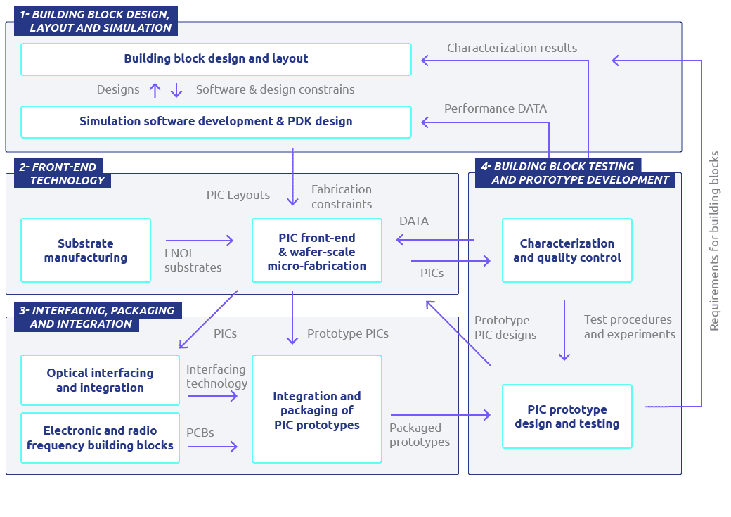
The graph visualises how ELENA’s various activities intertwine to produce the project results.
The dark blue boxes mark ELENA’s four main research areas. For the moment, you can find out about the detailed objectives of each area (section below). As ELENA progresses over time, you will find the most important results of these four areas on this page.
The easiest way to stay up to date is to subscribe to ELENA’s newsletter! Issue #1 is to be expected by the end of 2022.
Objectives
- Obtain detailed specifications for all building blocks (BBs) based also on end-user and prototype requirements;
- Conceive the roadmap for the BB development from the first simulations to final PDK (Process Design Kit);
- Optimized design of BBs using 2D and 3D simulations;
- Transfer of the design into GDS (Graphic Design System) layouts compatible with the fabrication process;
- Validation of design and simulations against measurements and improvements if necessary;
- Implement system-level simulation of a PIC produced with these BBs;
- Provide open access to the developed BBs by implementing a PDK (industry standard).
Subscribe to our newsletter to stay tuned about ELENA’s results.
Objectives
- Build a wafer-scale micro-fabrication technology for low-loss (<0.2dB/cm) LNOI optical passive components (e.g., waveguides, resonators, beam splitters);
- Develop the fabrication process flow for active BBs that allows two-layer metallization for electrical interconnection and deposition of a low-loss SiO2 cladding (loss < 0.2dB/cm);
- Optimize the fabrication process to achieve target yield (> 60%) and target performance for passive and active BBs;
- Develop a chip release technology with polished facets for edge-coupling applications (IL < 2dB);
- Produce high-quality 150 mm LNOI wafers for integrated photonics applications with 500 nm LNOI thickness and 3 μm buried oxide (BOX) and maximum hetero- structure temperature compatibility up to 500°C (exploratory work will perform towards 600 nm and 5 μm BOX).
Subscribe to our newsletter to stay tuned about ELENA’s results.
Objectives
- Develop BB to interface ELENA LNOI PICs with single-mode fiber (SMF28) and InP chips based on in-situ 3D-printing;
- Develop and fabricate 3D-printed micro-optic arrays for optical testing of edge-coupled LNOI PICs;
- Develop and build electronic BB PCB (Printed Circuit Board) for low-frequency control and tuning of optical building blocks;
- Assemble LNOI PICs, electronics and other parts required on a common carrier;
- Package the integrated PIC prototypes for testing.
Subscribe to our newsletter to stay tuned about ELENA’s results.
Objectives
- Component-level optical characterization of individual BBs (e.g., using probe stations) to provide experimental feedback on design and fabrication (including passive BBs, low-frequency and RF response of active BBs);
- Higher-level testing of BBs (including test of monolithic integration of few BBs on simple test PICs, test on Printed Wiring Board (PWB) and associated losses and test using standard Printed Circuit Board (PCB) and providing feedback on design and fabrication;
- Assessment of reliability and acquiring the statistical experimental data to build the PDK library;
- Conceiving, designing and simulating the prototype device using ELENA’s BB library;
- Testing of the prototype devices.
Subscribe to our newsletter to stay tuned about ELENA’s results.


